EMI Absorber: Enabling Reliable Wireless Performance
As modern electronic devices continue to become thinner, faster, and more integrated, electromagnetic interference (EMI) has become one of the most critical challenges affecting wireless communication performance, certification compliance, and product reliability. EMI absorbers provide an effective solution by suppressing unwanted electromagnetic noise while improving signal quality across multiple applications such as NFC, wireless charging, GPS modules, payment terminals, and industrial computing systems.
This article highlights how EMI absorber technology helps manufacturers overcome design limitations and accelerate product certification and time-to-market.
What Is an EMI Absorber?
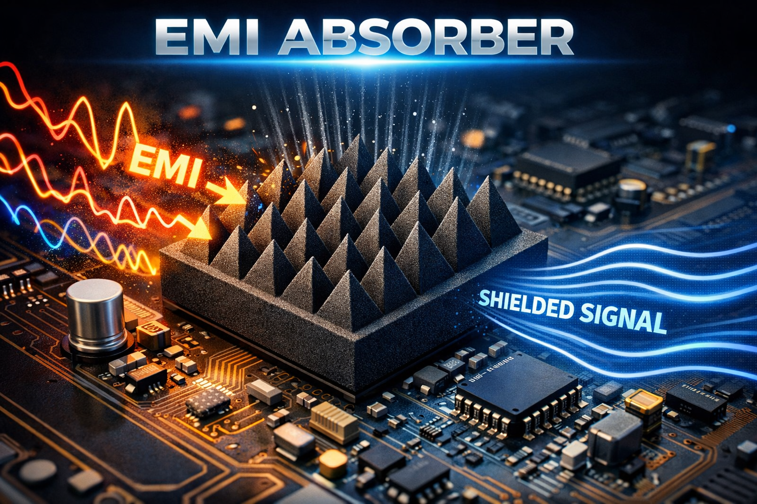
An EMI absorber is a high-permeability material designed to absorb electromagnetic radiation and convert unwanted noise energy into thermal energy. Unlike traditional shielding that reflects interference, absorbers suppress noise at the source, making them especially useful in compact electronic structures where reflections may worsen signal distortion.
Typical benefits include:
✅ Reduced radiated emission
✅ Improved antenna efficiency
✅ Enhanced signal stability
✅ Faster certification approval
✅ No PCB redesign required
Solving NFC Signal Shift Problems in Metal-Dense Devices
Near-field communication (NFC) systems operate at 13.56 MHz, but integration with Bluetooth antennas or nearby metal components often shifts the frequency and reduces reading distance.
In one deployment scenario, NFC performance failed strict 4 cm reading distance tests across seven reader platforms due to antenna interference. By integrating EMI absorber materials:
- Frequency shift was corrected from 16–20 MHz back to 13.56 MHz
- Signal strength improved through guided magnetic flux control
- Noise interference from surrounding components was absorbed effectively
- The device passed all compatibility requirements without redesigning the PCB or enclosure
This demonstrates how absorbers act as a fast corrective solution during late development stages.
Improving Wireless Charging Efficiency and Achieving Qi Certification
Wireless charging modules often suffer from:
- energy loss
- thermal buildup
- coil misalignment
- metal-induced magnetic interference
By introducing high-permeability wave absorbers:
- magnetic flux was redirected efficiently
- system temperature stability improved
- metal interference was suppressed
- strict WPC Qi certification requirements were successfully achieved
Ultra-thin absorber sheets also allowed seamless integration into slim phone housings and battery covers without increasing device thickness.
Passing Radiated Emission Tests Without Hardware Redesign
Industrial PC systems and high-density electronics frequently fail radiated emission testing due to internal high-frequency noise coupling.
Strategic absorber placement on:
- FPC/FFC cables
- core chips
- high-noise radiation paths
resulted in:
📉 significant emission reduction across frequency bands
📈 successful compliance with industrial radiation standards
🚀 elimination of costly PCB redesign cycles
This approach enables manufacturers to maintain project schedules even after EMI failures during certification stages.
Enhancing GPS Signal Accuracy in Noisy Electronic Environments
GPS antennas are extremely sensitive to internal device noise, especially within the 100 MHz–1 GHz range.
Applying absorbers around antenna structures:
- reduced internal noise floor
- increased signal strength beyond 40 dB
- shortened Time-to-First-Fix (TTFF)
- improved positioning accuracy in dense RF environments
These improvements are essential for navigation systems, tracking devices, and smart mobility applications.
Enabling Reliable NFC Operation Inside Metal Laptop Structures
Metal housings and battery packs often generate eddy currents that degrade NFC communication performance.
With ultra-thin absorber sheets (0.05–0.1 mm):
- magnetic flux was guided efficiently between antenna and metal surfaces
- reading distance improved to 5–10 cm
- ISO 18092 and EMV certification requirements were satisfied
This solution ensures secure authentication and seamless tap-to-pair connectivity even in slim notebook designs.
Supporting Payment Terminal Certification and Transaction Stability
Payment terminals must comply with strict certification standards such as:
- PCI PED
- EMV L1 / L2
Absorbers helped eliminate multi-band interference generated by tightly integrated wireless modules, enabling:
🔒 stable card detection
📡 uninterrupted wireless communication
⚡ faster approval during certification testing
This improves both transaction reliability and end-user experience in retail environments.
Improving High-Speed Reader Performance in Compact Systems
Compact smart card readers operating at 13.56 MHz often suffer from signal instability caused by nearby processors and metal surfaces.
Precision EMI absorption solutions provided:
- cleaner RF signal environments
- improved transaction success rates
- stable 848 kbps data transmission
- compatibility with MIFARE and FeliCa platforms
These advantages are critical for transportation, identity verification, and secure access systems.
Key Advantages of EMI Absorber Integration
Across all applications, EMI absorbers consistently deliver:
✔ faster certification approval
✔ improved antenna sensitivity
✔ reduced development risk
✔ better thermal stability
✔ thinner and lighter product designs
✔ cost savings compared with metal shielding redesign
Most importantly, they allow engineers to solve EMI problems without changing PCB layout or mechanical structure, making them ideal for late-stage optimization.
Please contact GlueRu to provide solutions to your challenges!